Modern electronics demand test strategies that are not only accurate but efficient. Our Design for Testability (DFT) approach integrates test considerations directly into the product development phase, ensuring that every fixture, layout, and component is optimized for accessibility and coverage.
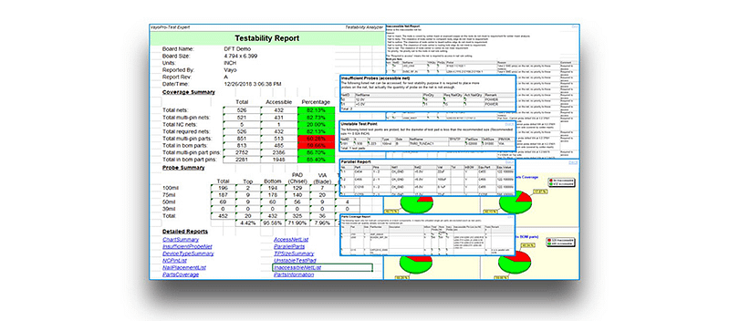
Comprehensive diagnostics to evaluate product accessibility for various test methods across 13 distinct rule categories
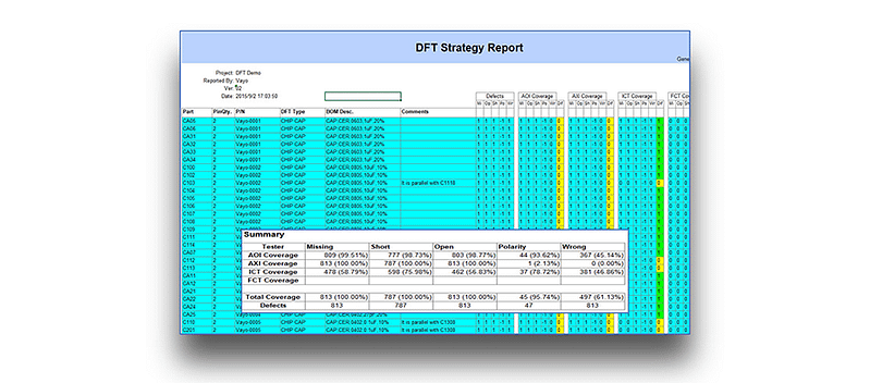
Detailed breakdown of defect coverage across different test technologies to improve yield and shorten debug cycles
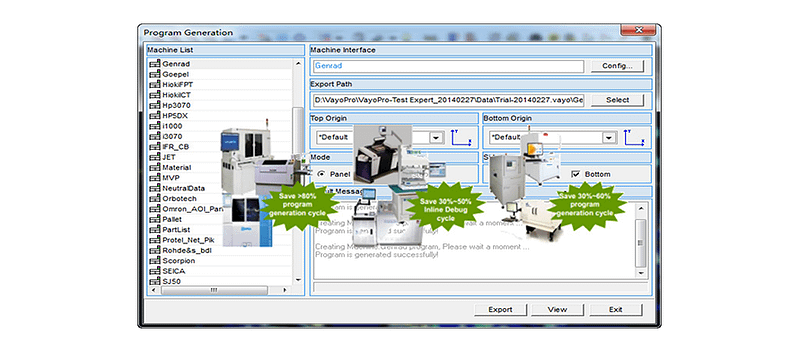
Output generation for integration into downstream testing and inspection systems, boosting NPI readiness
ICS Engineering partners with leading industry consultants to deliver advanced JTAG/Boundary Scan test solutions for high-complexity electronics across Southeast Asia.
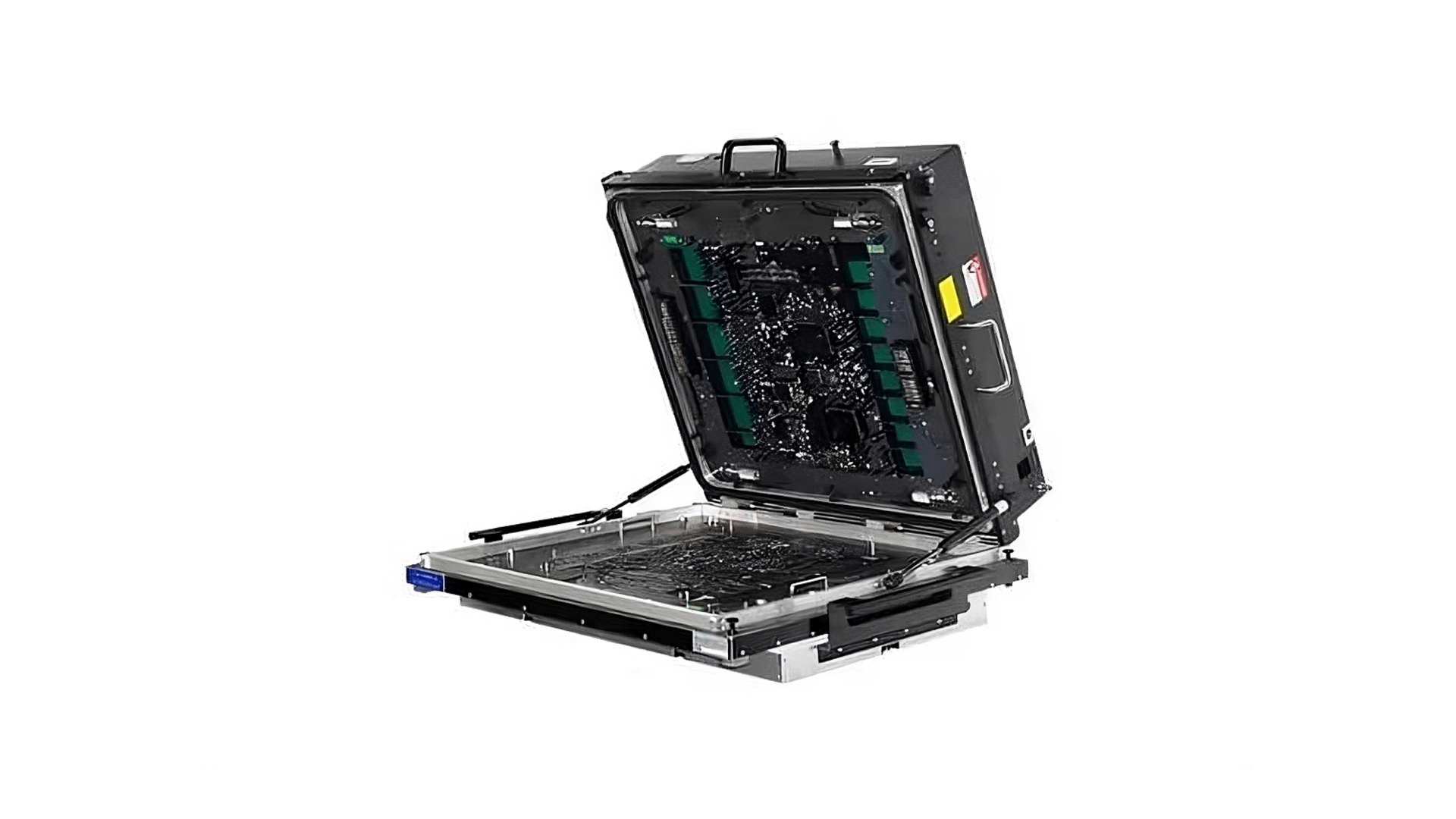
We perform digital, static testing of pin networks on embedded circuit boards — including access to I²C and SPI components. Our boundary scan methods evaluate processor inputs, dynamic memory, and high-speed interfaces (e.g. USB 3.0) to detect structural faults early and accurately.
Our advanced JTAG tools support on-board programming of serial (I²C, SPI) and parallel Flash memory (NOR, NAND). This includes writing directly into on-chip memory across FPGAs, SoCs, and microcontrollers — enabling scalable parallel programming during production.
We integrate functional test routines directly into boundary scan operations. From analog signal measurement to dynamic memory validation, our solutions extend fault coverage for components that are otherwise inaccessible through traditional probe methods.
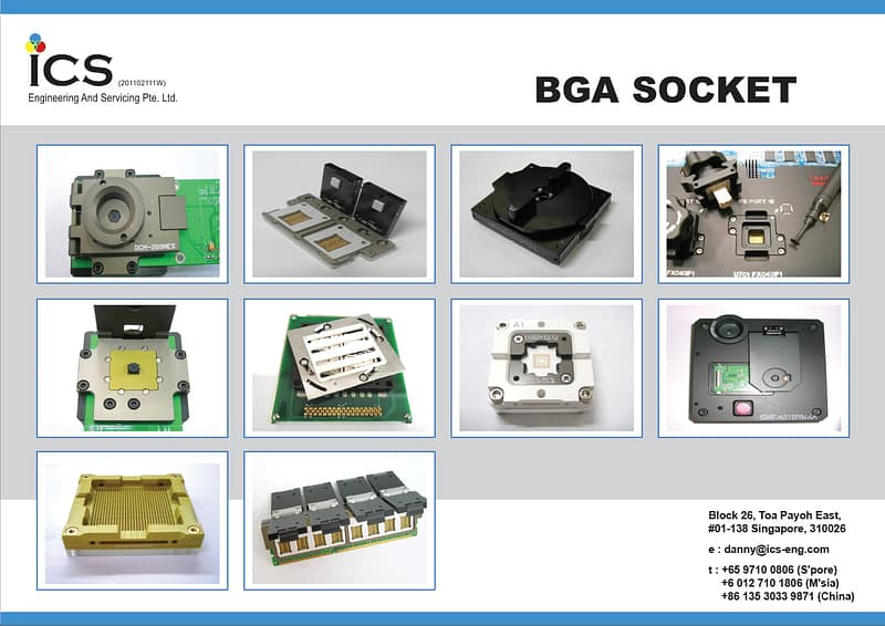
Whether you need a custom test fixture or a full automation solution, our engineers are ready to help you scale with speed, precision, and confidence.
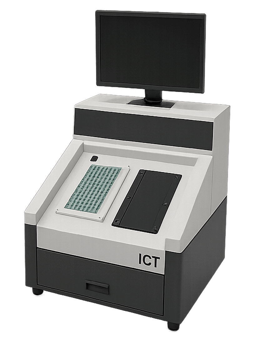
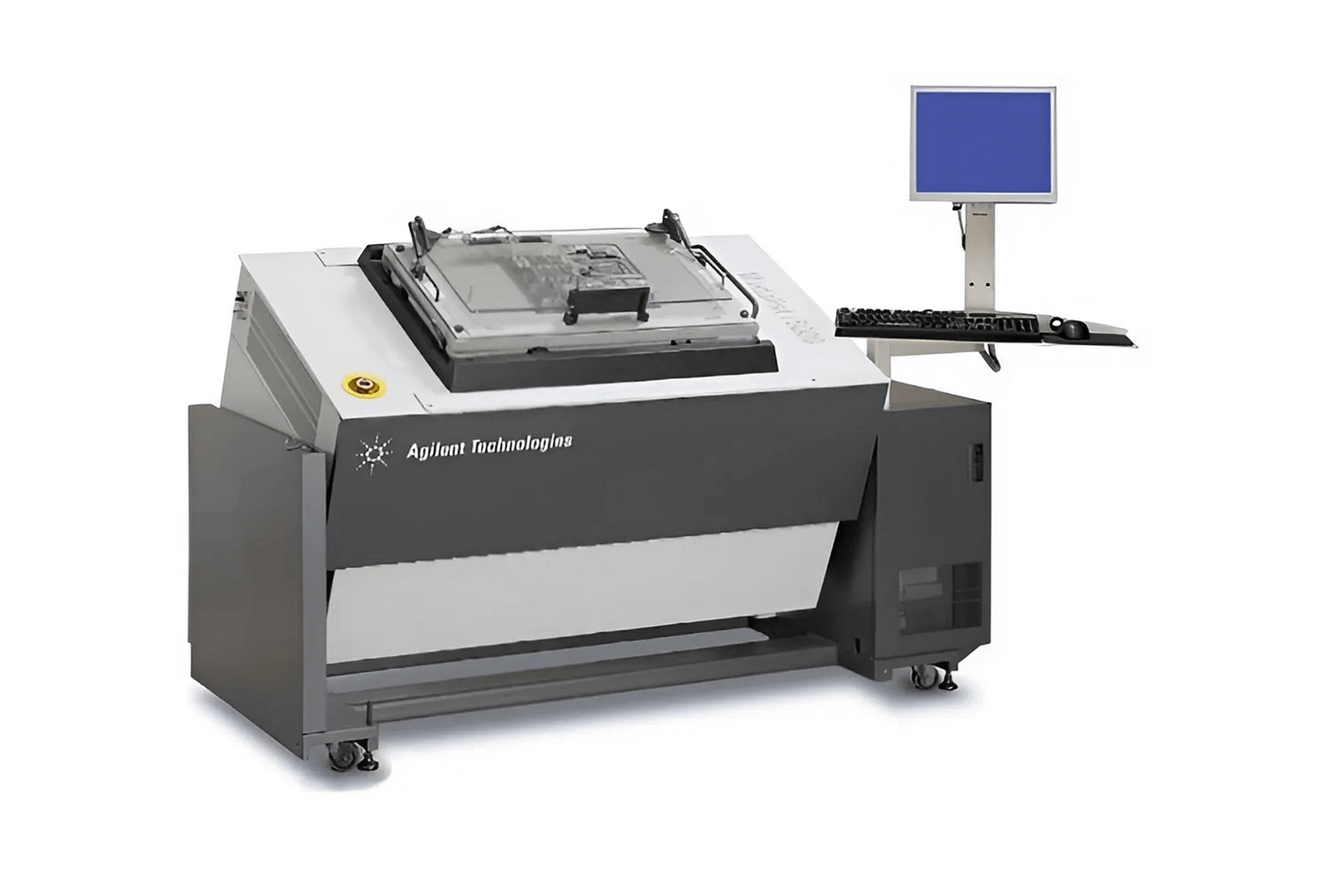
From test fixtures to turnkey automation, ICS Engineering & Servicing Pte Ltd delivers solutions that power Southeast Asia’s electronics and manufacturing industry.